
Principle of Operation
Linear Scan
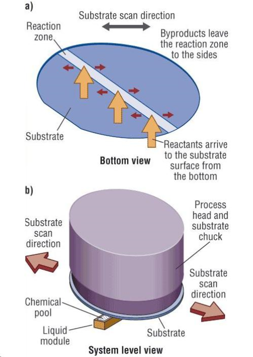 Fig. 1. WaveEtch Linear Scan schematic
The key technology behind the WaveEtch's outstanding single-sided etching performance is called LinearScan. LinearScan etching technology provides high uniformity as well as single-sidedness on ultra-thin large substrates. It also provides a consistent and uniform supply of chemicals throughout the liquid-solid interface while making available an orthogonal path for the byproducts, such as gases and vapors (Fig. 1a). The fact that every surface element is exposed to the same chemical and transport environment makes the process intrinsically uniform. The boundary layer is not subject to speed gradients, convection, or other transport-related gradients that may cause variations in its thickness and its concomitant impact on uniformity. The system eliminates virtually all transport-related and centrosymmetrical nonuniformities, which plague spin/spray or immersion processes.
The substrate is held on the nonprocess side by conventional vacuum or noncontact chucking alternatives, while it is gently scanned over a narrow pool of chemicals (Fig. 1b). The reactants enter the reaction zone through the bottom, and the byproducts exit in a plane parallel to the substrate surface. The substrate is not immersed, but merely put in contact with the top of the pool’s meniscus (Fig. 2). The chemicals and vapors are kept away from the nonprocess side by a proprietary technology called Dynamic Confinement, which forms a virtual gaseous o-ring around the periphery of the substrate to prevent any liquid or vapor incursion. In this way, the nonprocess side is not subject to physical or chemical contact.
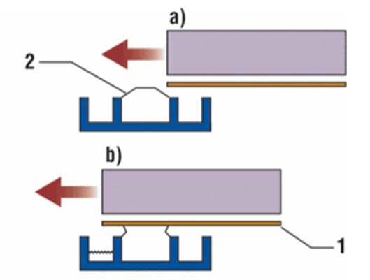 Fig. 2. WaveEtch Linear Scan Process Schemcatic
Because the system enables material removal uniformity, it allows more chemical material removal while staying within the uniformity budget. One such typical step is subsurface damage removal after grinding. For a given final thickness, the substrate can be ground to a thicker state and more material removed chemically while still staying within the uniformity budget. Grinding to a greater thickness increases the yield and reduces the overall cost of the operation.
The final thickness for modern IC devices continues to decrease, with 50μm being the current state-of-the art target for many modern devices. The described etching systems are particularly well suited to handle and process very thin wafers. The unique chucking and etching occurs with no violent spinning, no need for lateral confinement by pins or other hard devices that may damage the wafer’s edge, and no dynamic loading due to high rotational speeds.
The technology also allows for flexible tools for chemical surface treatments. Since there is no need to tailor the chemistries to stabilize the boundary layer over the large radial speed gradients present in spin/spray systems, there is a lot of freedom in chemistry choice. A given chemistry is only chosen for its desired surface interaction and not for any other ancillary reason, which typically conflicts with, or hinders the achievement of, the desired results.
Flexible chemical choice and the absence of large surface flow speeds, which tend to delete pre-existing surface features, allow multiple chemical steps to be superimposed to achieve additive surface features. For instance, nano-roughness can be superimposed over a micro-rough surface, which then provides an excellent surface for metal adhesion and other processes.
In the absence of hydrodynamic edge effects, the edges of the wafers are free of edge sharpness and the formation of “teeth,” features common in spin/spray etch systems that significantly weaken the substrates (Fig. 3). Also, the chemistries used do not require surfactants and are used in smaller volumes at lower flow rates, allowing for more efficient chemical usage. Chemicals can be used to a process-dictated end-point without regard to surfactant depletion. Together, these features lower chemical usage and its associated purchase and disposal costs, as well as often easing environmental regulatory compliance, resulting in overall production and costs-of-ownership reduction.
These processes are size-independent. Since all areas are exposed to the same chemical and transport environment, the size and shape of the substrate are largely irrelevant. The same process that is developed for a given wafer size, can be readily used for another wafer size, thus making product process migration effortless and cost effective. Substrates of odd shapes, of noncircular shapes, and larger than 300mm can be accommodated by the system.
Contact Us Today!
MATECH
182 Old Route 9 Ste 1
Fishkill, NY 12524
Phone: +1 845 463-2799+1 845 463-2799
E-mail: info@matech.com
 WaveEtch: The Greenest Wet Etcher