
Linear Scan
"The patented LinerScan technology decouples transport phenomena from the etching process itself."
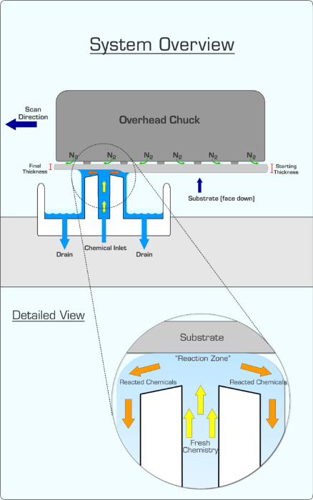 Fig. 1. LinearScan cross sectional schematic.
Only the WaveEtch offers an intrinsically uniform, size independent etching process. Its LinearScan technology "scans" a thin line of etchant across the surface of the wafer. Fig. 1. In the process, the chemistry and the wafer material react, removing material. These steps are repeated until the desired amount of material has been removed.
Notice that along the reaction zone "meniscus" there is no dependence on its length. Since the reactants arrive from below, and the byproducts leave the reaction zone through the sides, all areal elements being reacted experience the same environment: there is no size dependence. There are no areal elements which reactants or byproducts have to travel more or less than any other element in the reaction zone. The same is true for the rest of the wafer. These aspects are true for any wafer size; the same process results are obtained on a 4" wafer than in a 12" wafer. See Fig. 2 for typical uniformity results during the removal of 75 um of silicon 4", 6", and 8" wafers.
This unique feature of the WaveEtch's LinearScan technology effectively decouples all transport phenomena from the chemical process allowing it to take place uniformly all across the reaction zone and the wafer.
 Fig. 2. Etch uniformity across different Si wafer sizes.
Contact Us Today!
MATECH
182 Old Route 9 Ste 1
Fishkill, NY 12524
Phone: +1 845 463-2799+1 845 463-2799
E-mail: info@matech.com
 WaveEtch: The Greenest Wet Etcher